On Super-Fine Finishing of Optical Surfaces
Beaucamp Anthony
 Dear colleagues,
My name is Beaucamp Anthony, I joined the department of micro-engineering as Senior Lecturer in April 2015. I would like to take this opportunity to introduce my research and share with you some of my experiences since joining Kyoto University.
For the past 15 years, my research has been focused on achieving ever-finer surfaces by means of abrasive machining. The origins of this technology are very old, starting in pre-history with the burnishing of stones as tools and ornament, and advancing through the middle ages and renaissance with the introduction of grinding and polishing machines by the likes of Da Vinci and Galileo. One of the crucial application for surface finishing is in optics: Newton himself, well known for his research with prisms and thin films, was pushed into developing new techniques for polishing optical glass using natural pitch (a black, tar-like substance). Although he had no means of measuring it, Newton’s optics had micron level shape accuracy, and nanometer level roughness! It would take centuries for technology to progress much beyond this point, until the advent of computer controlled (NC) machines that improved process controllability, and presently allow us to reach down to nanometer level shape accuracy, and angstrom level roughness.

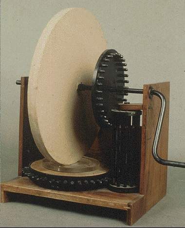
Mirror grinding machine, by Da Vinci
As in the days of Galileo and Newton, astronomical, medical and particle physics researchers are beholden to the engineers who deliver the optical components required in the build of new observatories, measurement equipment, etc. For example, high energy radiations such as X-rays and gamma rays, which are emitted by supernovas and black hole accretion discs, but also generated inside synchrotrons, have nanometer scale wavelength. To focus such radiation, the specification for shape accuracy and surface roughness is very tight, in the order of few atoms of deviation. To achieve such level of accuracy, a tight combination of skills is required: (1) Ultra-precise metrology, that is the ability the measure artifacts with an absolute accuracy of 1 part in 109 (typically: 1nm accuracy over 1m distance). (2) Material science, that is an understanding of material removal mechanisms at the molecular level, in order to machine substrates with atomic resolution. (3) Automation science, that is the ability to design tools and machines to can deliver the process in a controllable and repeatable fashion.


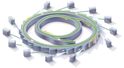
Applications of super-fine surfaces (top: synchrotron, bottom: black hole)
Although optical fabrication was long regarded as a critically important technology in Europe, the United States, and also Japan, in recent years the number of master opticians in these countries has steadily decreased, and much of the know-how is moving to south-east Asia. However, Japan is well placed to retain much of this core technology. Innovative research is still going strong at many universities across the country, and since coming to Japan (first in Nagoya and now in Kyoto), I have had the chance to meet and collaborate with numerous researchers across industry and academia. Their support, through collaborative research, as well as loaning of state-of-the-art equipment, has been outstanding. In return, it is with great pleasure that I now teach our research students the know-how and methodologies of optical fabrication, which were passed down from my mentors, and can make it through to the next generation of engineers who will take charge of designing and fabricating the optical systems powering our technological future.
(講師 マイクロエンジニアリング専攻)
